Paper Link
View Project Paper ISSCC format
Design choice:
To address the limitations of the ripple carry, carry lookahead, and carry save adders, we selected the parallel prefix adder (PPA) architecture. PPA reduces carry propagation delay by using a tree-like structure that computes carries in parallel, significantly shortening the critical path and improving speed.
We explored two well-known PPA variants, the Brent-Kung and Kogge-Stone adders. The Brent-Kung adder is more power-efficient and compact, making it well-suited for large bit-widths. However, its deeper logic tree limits speed [7]. The Kogge-Stone adder is one of the fastest architectures due to minimal logic depth and fan-out, but this comes at the cost of increased area.
For logic style, we chose dynamic logic over static CMOS and pseudo-NMOS. Dynamic logic uses fewer transistors (N+2 vs. 2N for static CMOS), offers smaller load capacitance, no static power, and faster switching—typically 1.3–2× faster. However, it also introduces challenges such as higher power consumption, charge sharing, and noise sensitivity. To mitigate these, we included keeper transistors, additional precharge control, and used domino logic. Since our design goal was to optimize for speed, these tradeoffs were acceptable and aligned with our performance priorities.
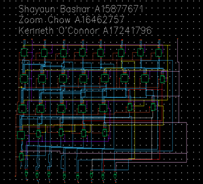
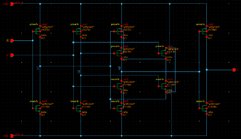
KSA Blocks:
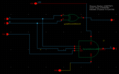
Propagate-Generate Cell:
The Propagate-Generate Cell (PG Cell) is a crucial component among the three distinct cells employed in the construction of our 8-bit Kogge-Stone adder. This cell serves as a pre-processing stage, responsible for computing generate and propagate signals for each pair of input bits, denoted as A and B. The generation of these signals follows a well-defined logic, governed by the following equations:
pi = Ai ⊕ Bi
gi = Ai · Bi
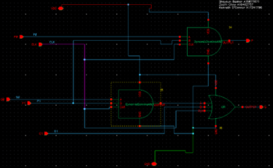
Fundamental Carry Operator Cell:
The Fundamental Carry Operator Cell (FCO Cell) serves as the second key component within our 8-bit Kogge-Stone adder. It can be conceptualized as a block comprising a group propagate and generate structure, or as a carry look-ahead network. These intermediate signals, denoted as group propagate and generate, play a pivotal role in the adder’s operation, and are determined by the following logic equations:
Pi:j = Pi:k+1 · Pk:j
Gi:j = Gi:k+1 ∨ (Pi:k+1 · Gk:j)
Post Processing Carry Cell:
The Post Processing Carry cell (PPC Cell) is one halve of the third and final distinct cell to complete the construction of our 8-bit Kogge-Stone adder. This cell serves as a part of the post-processing stage, responsible for the carry out values given the P and G values from the prior FCO stage as well as the carry in. The signals can be illustrated with the following logic equation:
Ci = (Pi · Cin) ∨ Gi
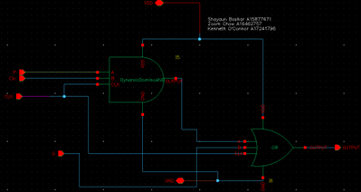
Post Processing Sum Cell:
The Post Processing Sum Cell (PPS Cell) is the second halve of the third and final distinct cell to complete the construction of our 8-bit Kogge-Stone adder. This cell serves as a part of the post-processing stage, responsible for the output of the sum values. The signals can be illustrated with the following logic equation:
Sumi = pi ⊕ Ci-1
OR + AND transistor Level Implementation with Dynamic & Domino Logic + High Skew Inverter:
AND Gate:
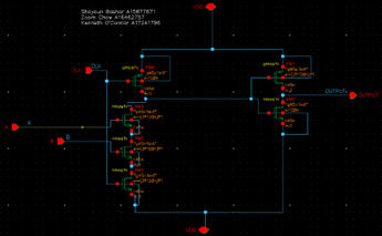
Shows the transistor level implementation of the AND gate found in the PG, PPC and FCO cell. This gate is utilizing dynamic and domino logic, giving way to faster operation. We have placed a high-skew inverter at the output of the AND gate to favor a rising edge transition to be able to take advantage of the lower logical effort needed for the gate.
OR Gate:
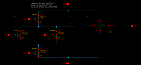
Shows the transistor level schematic of the OR gate utilizing dynamic and domino logic to provide lower logical effort and therefore faster operation. The OR gate is found in multiple cells that are crucial for the operation of the 8-bit adder such as the PPC and FCO cell. This custom designed gate also utilizes a high skew inverter, favoring a critical rising edge on the output, and using less logical effort compared to an un-skewed inverter.
Transisent simulation and Results:
Automatic place and route ripple carry adder vs. Kogge-Stone Adder:
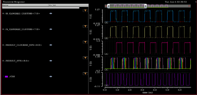
Automatic Place and Route Adder simulation at fMax=2.2Ghz
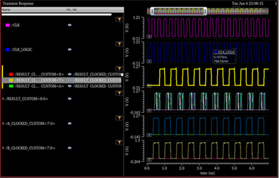
Kogge-Stone Adder at fMax=3Ghz
Table Results:
| Category | Place+Route Schematic | Custom Design Schematic | Place+Route (Optional) | Custom Design (Optional) |
|---|---|---|---|---|
| Performance for VDD = 1.1V | ||||
| fmax | 2.2 GHz | 3 GHz | NA | NA |
| Power consumption @ fmax | 529 µW/cycle | 78.64 µW/cycle | NA | NA |
| Energy per operation @ fmax | 240.5 fJ/cycle | 26.9 fJ/cycle | NA | NA |
| Performance for VDD = 1.1V, fCLK = 1 GHz | ||||
| Power consumption @ 1 GHz | 267 µW/cycle | 29.12 µW/cycle | NA | NA |
| Energy per operation @ 1 GHz | 267 fJ/cycle | 29.12 fJ/cycle | NA | NA |
| Other Important Parameters | ||||
| Adder architecture | Ripple-carry | Kogge-Stone Parallel Prefix | NA | NA |
| Core area | — | — | NA | NA |
| Critical input pair (A=?, B=?) | A = 00000001, B = 00111111 | A = 00000001, B = 00111111 | NA | NA |
| Transistor types used | Normal Threshold Voltage | Normal Threshold Voltage | NA | NA |
References:
References:
[1] https://www.diva-portal.org/smash/get/diva2:19722/fulltext01
[2] https://iopscience.iop.org/article/10.1088/1742-6596/1049/1/012077/pdf
[3] https://www.cl.cam.ac.uk/research/srg/han/ACS-P35/8-bit-KoggeStone-Adder.pdf
[4] https://www.youtube.com/watch?v=ivry9K_7HzM
[5] https://www.youtube.com/watch?v=tgY4UIufLd0
[6] https://link.springer.com/chapter/10.1007/978-1-4757-3705-94
[7] https://www.researchgate.net/publication/336825176 Comparitive_Analysis_of_Brent-Kang_Kogge-Stone_Parallel-Prefix_Adder_for_Their_Area_Delay_Power_Consumption
[8] http://www.ijeetc.com/v3/v3n1/13A0141(p.116-121).pdf
Project Team Members: Zoom Chow | Kenneth O’Connor | (ECE 165 Digital Integrated Circuit Design, UC San Diego, Prof. Patrick Mercier)